
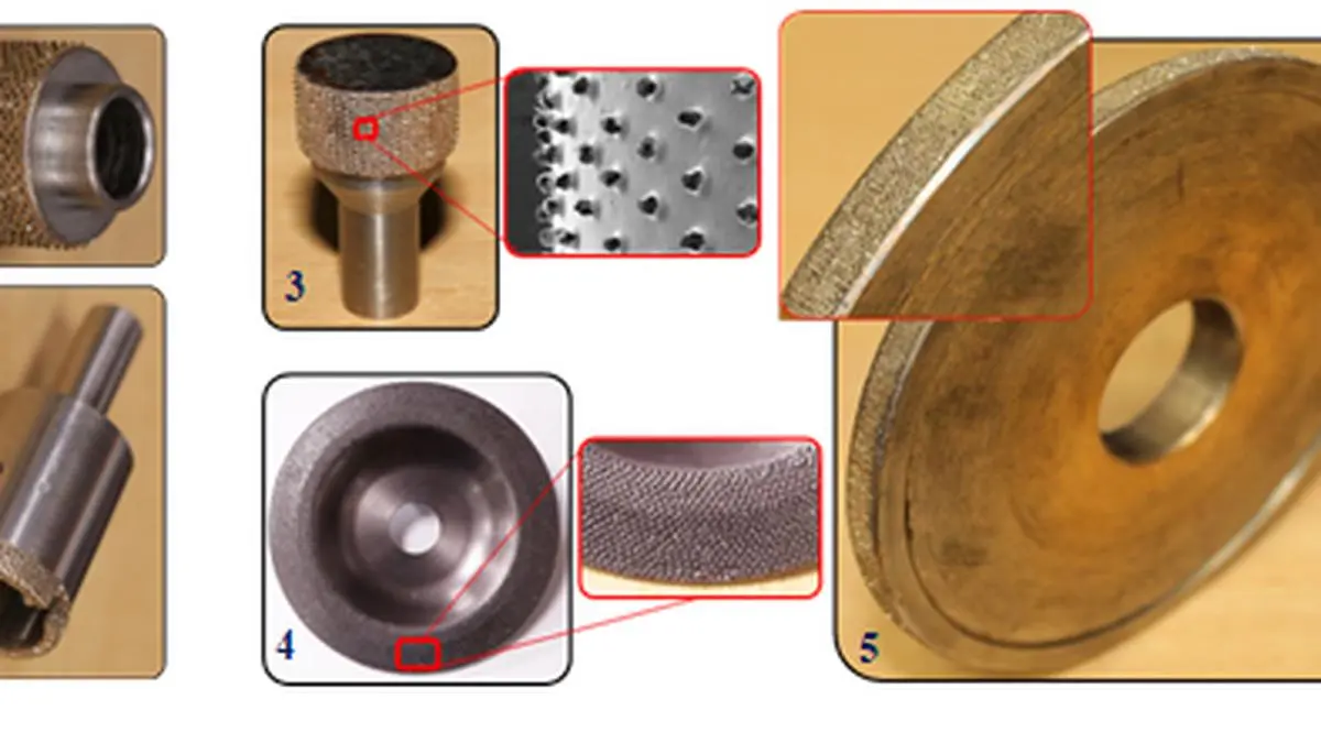
A new technology that can produce a new-generation of multi-point/single-layer, superabrasive tools for advanced grinding applications to meet high productivity and energy-efficient material removal requirements, has been developed by a research team headed by Dr Amitava Ghosh of IIT Madras. These tools also have an enhanced tool life. The team used advanced chemical bonding technology with an application-specific novel formulation of filler material and controlled spacing of grits on the tools by using an indigenously developed semi-automatic grit-printing machine.
The team recommends using application-specific advanced coatings to develop such new-generation superabrasive tools. This novel formulation offers an excellent blend of strength, wear resistance, and wetting characteristics (the ability to spread well in a liquid state with low contact angle during brazing). The grit-planting (planting/placing of grits in a pre-defined co-ordinate position on grinding wheel’s working surface) setup allows a manufacturer to print the grits in customised pattern to suit the requirement of an application. The recommended coating enhances the durability of the bond thus adding life to the developed tools.
These tools can be produced using active brasing technology with striking attributes of high crystal exposure above the bond level. The joint strength and wear-resistant characteristics of the bonds in these tools are superior to those of their commercial counterparts. These tools can withstand more grinding force, offer significantly higher tool life, and execute load-free grinding of advanced materials with extremely high material removal rates, says a press release.
2D nanos for low cost LCDs
A new easier technique of manufacturing liquid crystal displays (LCDs) which can reduce the cost of the devices has been developed. An essential requirement of these LCDs is the uni-directional planar alignment of the constituent liquid crystals (LC) over large areas.
Although the conventional polymer rubbing method yields quality LC alignment, it possesses unavoidable and undesirable drawbacks such as production of electrostatic charges and dust particles that interfere with display operation, and even cause damage to the electronic components of the display. While electrostatic charges increase the failure rate, dust creates defects which seriously compromises with the performance of the device. Other problems include multistep process for coating and the necessity for high-temperature curing. This has led to a surge in demand to replace this rubbing method with new non-contact techniques.
The latest among these techniques is to employ 2D nanomaterials — graphene, hexagonal boron nitride (h-BN), transition metal dichalcogenides, and so on — as alignment layers. But this requires high deposition temperature, precursors and yields hazardous by-products. Besides, when the CVD method is used, unidirectional LC alignment is observed over only small regions.
A team of scientists from the Centre for Nano and Soft Matter Sciences (CeNS), Bengaluru, has developed a novel way of employing 2D materials to overcome the drawbacks of current methods. Using h-BN nanoflakes as the specific material, the group comprising Gayathri Pisharody, Priyabrata Sahoo, Dr DS Shankar Rao, Dr HSSR Matte and Dr S Krishna Prasad employed a solution-processed deposition technique and found it to be effective in getting the LC alignment over a much larger area. They also found the resultant crystals to be quite robust with no evidence of decay in LC orientation over several months.
![]() Comments
Comments


Comments
Comments have to be in English, and in full sentences. They cannot be abusive or personal. Please abide by our community guidelines for posting your comments.
We have migrated to a new commenting platform. If you are already a registered user of TheHindu Businessline and logged in, you may continue to engage with our articles. If you do not have an account please register and login to post comments. Users can access their older comments by logging into their accounts on Vuukle.